Menu:
Rugged Data Logger
Description
The goal of this project was to develop the system architecture for a single-channel, rugged, low cost data logger for use in harsh electrical conditions. The rugged data logger can be used in electromagnetic compatibility (EMC) test setups or other harsh environments (electric power substations, industrial facilities) to provide robust data monitoring. EMC tests and other electrical transient occurrences are typically too severe for standard data logger equipment to survive without special decoupling methods.

Harsh electrical transients can disable standard measurement equipment, motivating the need for a robust data logger
Robustness is achieved by completely isolating the analog input from the rest of the data logger, and by using EMI filters at the analog front-end. Complete documentation of the specifications, system architecture block diagram, analog subsystem, PCB floor plan, and test plan can be found here (.pdf). A summary of this information is given in the Details section on this page.
This project gave me an opportunity to design the full architecture for an embedded system. I selected the microcontroller, memory, ADC, communication interface, and power distribution system to meet the requirements of the data logger. I also designed the full analog front end up to the ADC.
Project Takeaways
This project allowed me to gain technical experience in the following areas:
- Embedded system architecture design
- Microcontroller selection
- System memory selection
- Analog front-end design
- Schematic capture using ExpressPCB
- Power rail distribution and power budgeting
- PCB floor planning and stackup
- Generating test plans to verify system and circuit functionality
- Component selection for cost-sensitive designs
Details
Data Logger Specifications
These are the specifications for the data logger.
- The data logger is a standalone device that has a power input, a single analog input (signal and return wire pair), and a communications port to access the data
- Measurement data shall be locally stored and have enough storage memory to hold 24 hours of data
- The incoming analog signal must be converted to 14-bit digital values at a 10kHz sample rateAnalog signal bandwidth of 1.2kHz, and = 10dB of attenuation at 5kHz (the frequency at which aliasing begins to occur)
- Accept an input analog signal range of -1V to 1V
- Power itself off an input power supply voltage ranging from 18 to 36VDC
- Must be isolated from input power supply
- Have an average power consumption of 500mW maximum
- Able to withstand harsh EMI events such as radiated and conducted high frequency interference and electrical transients
- Low cost
Architecture Block Diagram
A block diagram of the data logger architecture is shown below.
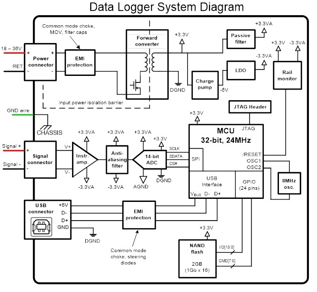
The analog signal pair is landed on a connector, routed through the analog front-end, and converted to a 14-bit digital value by an ADC operating at a sample rate of 10kSPS. The 14-bit samples are transmitted to a microcontroller (MCU) through an SPI interface. The MCU is the 32-bit PIC32MX250F256H-I/PT sold by Microchip. It collects sample data in temporary internal SRAM and then writes it to permanent external NAND flash storage. A USB interface is used to access and download the data on a separate device. Input power is isolated and stepped down using a forward converter to generate the +3.3V rails that power all the devices on the board.
A description of each sub-block and an analysis verifying that the architecture meets the requirements is given in the full documentation of the project.
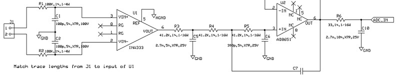
Analog Front-End
The analog front-end is implemented with a Texas Instruments INA333 instrumentation amplifier that converts the differential input voltage to a single-ended output voltage. An active anti-aliasing filter with a corner frequency of 1.23kHz, centered around an Analog Devices AD8651 op-amp, is used to filter the signal. A Texas Instruments ADC141S626 convers the filtered signal to a digital 14-bit value.
The full schematic and BOM for the analog front-end are given in the project documentation.
PCB Floor Plan
The PCB layout for the data logger board is shown below. Each component block in the figure is to scale; part dimensions were taken from datasheets of the selected parts. Components have not been selected for the power conversion circuits, so the Forward Converter Area in the figure shows the expected amount of area that will be taken by the power supply.
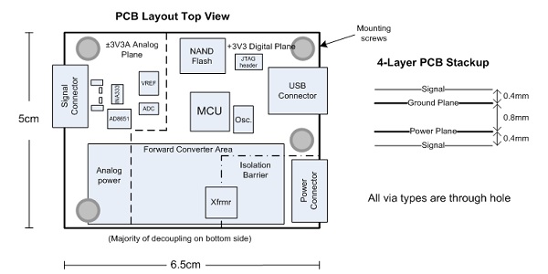
The layout is implemented on a 4-layer PCB that measures 5cm x 6.5cm. The proposed 4-layer stack up allows the signals to be tightly coupled to the ground and power planes, reducing current loop area.